1 of 44
REV: 040104
Note: Some revisions of this device may incorporate deviations from published specifications known as errata. Multiple revisions of any device
may be simultaneously available through various sales channels. For information about device errata, click here:
www.maxim-ic.com/errata
.
FEATURES
ß 80C52 Compatible
8051 Pin- and Instruction-Set Compatible
Four 8-Bit I/O Ports
Three 16-Bit Timer/Counters
256 Bytes Scratchpad RAM
ß Large On-Chip Memory
16kB Program Memory
1kB Extra On-Chip SRAM for MOVX
ß ROMSIZE Feature
Selects Internal ROM Size from 0 to 16kB
Allows Access to Entire External Memory Map
Dynamically Adjustable by Software
Useful as Boot Block for External Flash
ß High-Speed Architecture
4 Clocks/Machine Cycle (8051 = 12)
Runs DC to 33MHz Clock Rates
Single-Cycle Instruction in 121ns
Dual Data Pointer
Optional Variable Length MOVX to Access
Fast/Slow RAM/Peripherals
ß Power Management Mode
Programmable Clock Source to Save Power
CPU Runs from (Crystal/64) or (Crystal/1024)
Provides Automatic Hardware and Software Exit
ß EMI Reduction Mode Disables ALE
ß Two Full-Duplex Hardware Serial Ports
ß High Integration Controller Includes:
Power-Fail Reset
Early-Warning Power-Fail Interrupt
Programmable Watchdog Timer
ß 13 Interrupt Sources with Six External
ß Available in 40-pin PDIP, 44-Pin PLCC, 44-Pin
TQFP, and 40-Pin Windowed CERDIP
ß Factory Mask DS83C520 or EPROM (OTP)
DS87C520
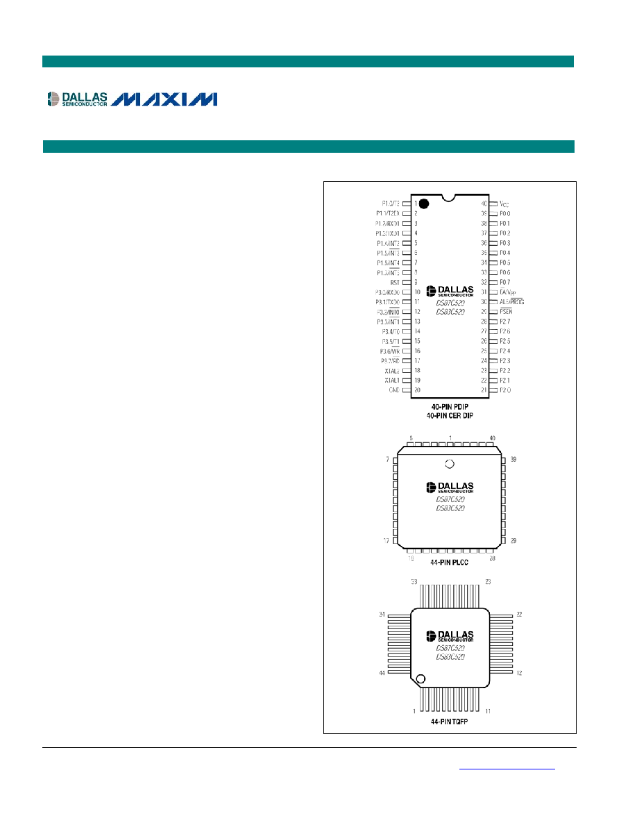
PIN CONFIGURATIONS
DS87C520/DS83C520
EPROM/ROM High-Speed Microcontrollers
www.maxim-ic.com
TOP VIEW
DALLAS is a registered trademark of Dallas Semiconductor Corp.
MAXIM is a registered trademark of Maxim Integrated Products, Inc.

DS87C520/DS83C520 EPROM/ROM High-Speed Microcontrollers
2 of 44
ORDERING INFORMATION
PART TEMP
RANGE
MAX. CLOCK
SPEED (MHz)
PIN-PACKAGE
DS87C520-MCL 0∞C to +70∞C 33
40
Plastic
DIP
DS87C520-QCL 0∞C to +70∞C 33
44
PLCC
DS87C520-ECL 0∞C to +70∞C 33
44
TQFP
DS87C520-MNL -40∞C to +85∞C 33
40
Plastic
DIP
DS87C520-QNL -40∞C to +85∞C 33
44
PLCC
DS87C520-ENL -40∞C to +85∞C 33
44
TQFP
DS87C520-WCL 0∞C to +70∞C
33
40 Windowed CERDIP
DS83C520-MCL 0∞C to +70∞C 33
40
Plastic
DIP
DS83C520-QCL 0∞C to +70∞C 33
44
PLCC
DS83C520-ECL 0∞C to +70∞C 33
44
TQFP
DS83C520-MNL -40∞C to +85∞C 33
40
Plastic
DIP
DS83C520-QNL -40∞C to +85∞C 33
44
PLCC
DS83C520-ENL -40∞C to +85∞C 33
44
TQFP
DESCRIPTION
The DS87C520/DS83C520 EPROM/ROM high-speed microcontrollers are fast 8051-compatible
microcontrollers. They feature a redesigned processor core without wasted clock and memory cycles. As
a result, the devices execute every 8051 instruction between 1.5 and 3 times faster than the original for
the same crystal speed. Typical applications will see a speed improvement of 2.5 times using the same
code and the same crystal. The DS87C520/DS83C520 offer a maximum crystal speed of 33MHz,
resulting in apparent execution speeds of 82.5MHz (approximately 2.5X).
The DS87C520/DS83C520 are pin compatible with all three packages of the standard 8051, and include
standard resources such as three timer/counters, serial port, and four 8-bit I/O ports. They feature 16kB of
EPROM or mask ROM with an extra 1kB of data RAM. Both OTP and windowed packages are
available.
Besides greater speed, the microcontroller includes a second full hardware serial port, seven additional
interrupts, programmable Watchdog Timer, Brownout Monitor, and Power-Fail Reset. The device also
provides dual data pointers (DPTRs) to speed block data memory moves. It also can adjust the speed of
MOVX data memory access from two to nine machine cycles for flexibility in selecting external memory
and peripherals.
A new Power Management Mode (PMM) is useful for portable applications. This feature allows software
to select a lower speed clock as the main time base. While normal operation has a machine cycle rate of 4
clocks per cycle, the PMM runs the processor at 64 or 1024 clocks per cycle. For example, at 12MHz,
standard operation has a machine cycle rate of 3MHz. In Power Management Mode, software can select
either 187.5kHz or 11.7kHz machine cycle rate. There is a corresponding reduction in power
consumption when the processor runs slower.
The EMI reduction feature allows software to select a reduced emission mode. This disables the ALE
signal when it is unneeded.
The DS83C520 is a factory mask ROM version of the DS87C520 designed for high-volume, cost-
sensitive applications. It is identical in all respects to the DS87C520, except that the 16kB of EPROM is
replaced by a user-supplied application program. All references to features of the DS87C520 will apply to
the DS83C520, with the exception of EPROM-specific features where noted. Please contact your local
Dallas Semiconductor sales representative for ordering information
.
The High-Speed Microcontroller User's
Guide must be used in conjunction with
this data sheet. Download it at:
www.maxim-ic.com/microcontrollers
.
DS87C520/DS83C520 EPROM/ROM High-Speed Microcontrollers
3 of 44
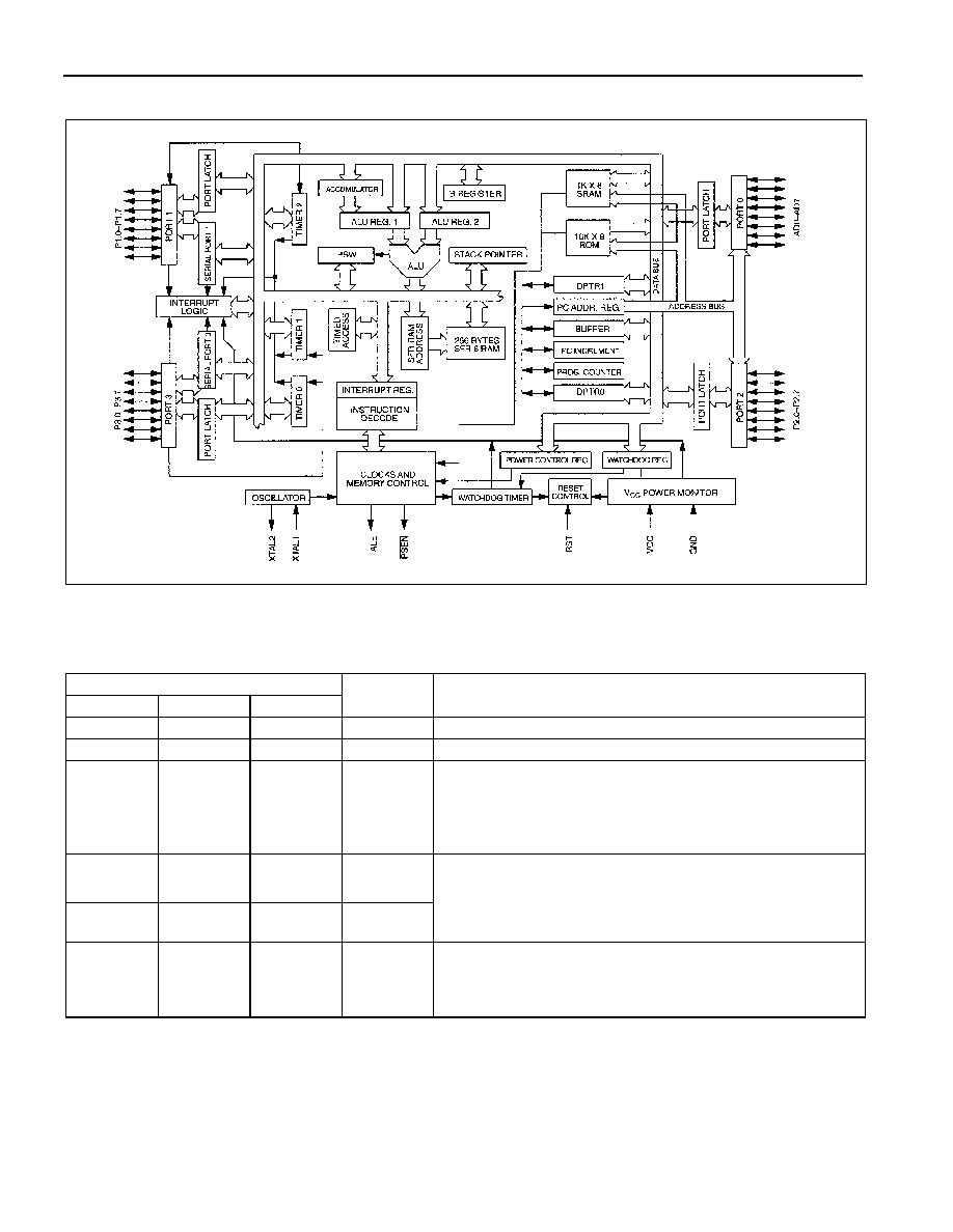
Figure 1. Block Diagram
PIN DESCRIPTION
PIN
DIP PLCC TQFP
NAME FUNCTION
40 44 38 V
CC
Positive Supply Voltage. +5V
20
1, 22, 23
16, 17, 39
GND
Digital Circuit Ground
9 10 4 RST
Reset Input. The RST input pin contains a Schmitt voltage input
to recognize external active high Reset inputs. The pin also
employs an internal pulldown resistor to allow for a combination
of wired OR external reset sources. An RC is not required for
power-up, as the device provides this function internally.
18 20 14
XTAL2
19 21 15
XTAL1
Crystal Oscillator Pins. XTAL1 and XTAL2 provide support for
parallel-resonant, AT-cut crystals. XTAL1 acts also as an input if
there is an external clock source in place of a crystal. XTAL2
serves as the output of the crystal amplifier.
29 32 26
PSEN
Program Store-Enable Output. This active-low signal is
commonly connected to optional external ROM memory as a chip
enable.
PSEN provides an active-low pulse and is driven high
when external ROM is not being accessed.
DS87C520/
DS83C520

DS87C520/DS83C520 EPROM/ROM High-Speed Microcontrollers
4 of 44
PIN DESCRIPTION (continued)
PIN
DIP PLCC TQFP
NAME FUNCTION
30 33 27 ALE
Address Latch Enable Output. The ALE functions as a clock to
latch the external address LSB from the multiplexed address/data bus
on Port 0. This signal is commonly connected to the latch enable of an
external 373 family transparent latch. ALE has a pulse width of 1.5
XTAL1 cycles and a period of four XTAL1 cycles. ALE is forced
high when the DS87C520/DS83C520 are in a reset condition. ALE
can also be disabled and forced high by writing ALEOFF = 1
(PMR.2). ALE operates independently of ALEOFF during external
memory accesses.
39 43 37
P0.0
(AD0)
38 42 36
P0.1
(AD1)
37 41 35
P0.2
(AD2)
36 40 34
P0.3
(AD3)
35 39 33
P0.4
(AD4)
34 38 32
P0.5
(AD5)
33 37 31
P0.6
(AD6)
32 36 30
P0.7
(AD7)
Port 0 (AD0≠7), I/O. Port 0 is an open-drain, 8-bit, bidirectional I/O
port. As an alternate function Port 0 can function as the multiplexed
address/data bus to access off-chip memory. During the time when
ALE is high, the LSB of a memory address is presented. When ALE
falls to a logic 0, the port transitions to a bidirectional data bus. This
bus is used to read external ROM and read/write external RAM
memory or peripherals. When used as a memory bus, the port
provides active high drivers. The reset condition of Port 0 is tri-state.
Pullup resistors are required when using Port 0 as an I/O port.
1 2 40 P1.0
2 3 41 P1.1
3 4 42 P1.2
4 5 43 P1.3
5 6 44 P1.4
6 7 1 P1.5
7 8 2 P1.6
8 9 3 P1.7
Port 1, I/O. Port 1 functions as both an 8-bit, bidirectional I/O port
and an alternate functional interface for Timer 2 I/O, new External
Interrupts, and new Serial Port 1. The reset condition of Port 1 is with
all bits at a logic 1. In this state, a weak pullup holds the port high.
This condition also serves as an input state; a weak pullup holds the
port high. This condition also serves as an input mode, since any
external circuit that writes to the port will overcome the weak pullup.
When software writes a 0 to any port pin, the DS87C520/DS83C520
will activate a strong pulldown that remains on until either a 1 is
written or a reset occurs. Writing a 1 after the port has been at 0 will
cause a strong transition driver to turn on, followed by a weaker
sustaining pullup. Once the momentary strong driver turns off, the
port again becomes the output high (and input) state. The alternate
modes of Port 1 are out-lines as follows.
Port Alternate
Function
P1.0
T2 External I/O for Timer/Counter 2
P1.1
T2EX EX Timer/Counter 2 Capture/Reload Trigger
P1.2
RXD1
Serial Port 1 Input
P1.3
TXD1
Serial Port 1 Output
P1.4
INT2
External Interrupt 2 (Positive Edge Detect)
P1.5
INT3
External Interrupt 3 (Negative Edge Detect)
P1.6
INT4
External Interrupt 4 (Positive Edge Detect)
P1.7
INT5
External Interrupt 5 (Negative Edge Detect)

DS87C520/DS83C520 EPROM/ROM High-Speed Microcontrollers
5 of 44
PIN DESCRIPTION (continued)
PIN
DIP PLCC TQFP
NAME FUNCTION
21 24 18
P2.0
(A8)
22 25 19
P2.1
(A9)
23 26 20
P2.2
(A10)
24 27 21
P2.3
(A11)
25 28 22
P2.4
(A12)
26 29 23
P2.5
(A13)
27 30 24
P2.6
(A14)
28 31 25
P2.7
(A15)
Port 2 (A8≠15), I/O. Port 2 is a bidirectional I/O port. The reset
condition of Port 2 is logic high. In this state, a weak pullup holds
the port high. This condition also serves as an input mode, since
any external circuit that writes to the port will overcome the weak
pullup. When software writes a 0 to any port pin, the
DS87C520/DS83C520 will activate a strong pulldown that
remains on until either a 1 is written or a reset occurs. Writing a 1
after the port has been at 0 will cause a strong transition driver to
turn on, followed by a weaker sustaining pullup. Once the
momentary strong driver turns off, the port again becomes both the
output high and input state. As an alternate function Port 2 can
function as MSB of the external address bus. This bus can be used
to read external ROM and read/write external RAM memory or
peripherals.
10 11 5 P3.0
11 13 7 P3.1
12 14 8 P3.2
13 15 9 P3.3
14 16 10 P3.4
15 17 11 P3.5
16 18 12 P3.6
17 19 13 P3.7
Port 3, I/O. Port 3 functions as both an 8-bit, bidirectional I/O
port and an alternate functional interface for External Interrupts,
Serial Port 0, Timer 0 and 1 Inputs, and
RD and WR strobes. The
reset condition of Port 3 is with all bits at a logic 1. In this state, a
weak pullup holds the port high. This condition also serves as an
input mode, since any external circuit that writes to the port will
overcome the weak pullup. When software writes a 0 to any port
pin, the DS87C520/DS83C520 will activate a strong pulldown that
remains on until either a 1 is written or a reset occurs. Writing a 1
after the port has been at 0 will cause a strong transition driver to
turn on, followed by a weaker sustaining pullup. Once the
momentary strong driver turns off, the port again becomes both the
output high and input state. The alternate modes of Port 3 are
outlined below.
Port
Alternate Mode
P3.0
RXD0
Serial Port 0 Input
P3.1
TXD0
Serial Port 0 Output
P3.2
INT0
External Interrupt 0
P3.3
INT1
External Interrupt 1
P3.4
T0
Timer 0 External Input
P3.5
T1
Timer 1 External Input
P3.6
WR
External Data Memory Write Strobe
P3.7
RD
External Data Memory Read Strobe
31 35 29
EA
External Access
Input, Active Low. Connect to ground to force
the DS87C520/DS83C520 to use an external ROM. The internal
RAM is still accessible as determined by register settings. Connect
EA to V
CC
to use internal ROM.
--
12, 34
6, 28
N.C.
Not Connected. These pins should not be connected. They are
reserved for use with future devices in this family.